

The journey into the nanoscale, a realm a thousand times smaller than a bacterium, represents one of the most profound scientific shifts of the late 20th century. For decades, the ability to directly see and manipulate individual atoms was confined to the realm of theoretical physics and science fiction, most famously articulated in Richard Feynman’s 1959 lecture, “There’s Plenty of Room at the Bottom.” This vision of building materials from the atom up remained a distant dream, blocked by the fundamental physical limitations of conventional microscopy. The transition from abstract concept to tangible reality required a two-part revolution. First, science needed new senses—tools that could not only visualize the atomic landscape but also interact with it. Second, armed with these new capabilities, scientists needed to discover and understand the unique building blocks that nature offered at this scale. The following sections chronicle this pivotal era, detailing the invention of the scanning probe microscopes that became the eyes and hands of nanoscience, and the subsequent discovery of a revolutionary family of carbon nanomaterials that provided the foundational toolkit for a new age of technology.
Section 3: The Tools of Creation: Inventing the Eyes and Hands of Nanoscience

For nanotechnology to transition from a conceptual dream to an experimental science, a fundamental barrier had to be overcome: scientists needed to be able to see and interact with the atomic world directly. For most of scientific history, this was impossible. Traditional optical microscopes, which use light to form images, are fundamentally limited by the diffraction of light, making it impossible to resolve features smaller than the wavelength of visible light (several hundred nanometers) [1]. While the invention of the electron microscope in the 1930s by Ernst Ruska and Max Knoll was a major leap forward, allowing for much higher magnification, it still could not routinely provide real-space images of individual atoms on a surface or, crucially, allow for their manipulation [2]. The world of the atom remained blurry and inaccessible. This changed dramatically in the 1980s with a paradigm-shifting invention that did not just improve upon existing microscopes but created an entirely new way of sensing the world. This invention gave science both the eyes to see and the hands to manipulate the atomic frontier.
The Scanning Tunneling Microscope (STM): A Quantum Leap
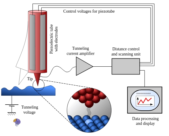
The Scanning Tunneling Microscope (STM) [19]
In 1981, at IBM’s Zurich Research Laboratory, physicists Gerd Binnig and Heinrich Rohrer, driven by a shared frustration with the inability to study surfaces at the atomic level, unveiled their groundbreaking invention: the Scanning Tunneling Microscope (STM) [3]. The STM’s operation was not based on light or high-energy electrons, but on a purely quantum mechanical phenomenon known as electron tunneling [4]. The principle is both elegant and powerful: a metallic tip, sharpened to the point of a single atom, is brought incredibly close—within a few angstroms (tenths of a nanometer)—to a conductive sample surface without physically touching it [5]. When a small voltage is applied between the tip and the sample, electrons can “tunnel” across the vacuum gap, creating a tiny but measurable electrical current [1].
This tunneling current is exponentially sensitive to the distance between the tip and the surface; a change in distance of just one atomic diameter can alter the current by a factor of 1,000 or more. Binnig and Rohrer harnessed this extreme sensitivity. By using piezoelectric actuators to scan the tip across the sample’s surface and a feedback loop to adjust the tip’s height to maintain a constant tunneling current, they could create a precise, three-dimensional topographic map of the surface, atom by atom [5]. On the night of March 16, 1981, they obtained their first clear images of the atomic structure of a gold crystal. As Binnig recalled, “It was entering a new world”[5]. The impact was immediate and profound. The STM provided the first direct, real-space images of atoms, translating the abstract quantum world into tangible, visual data. In recognition of the invention’s revolutionary importance, Binnig and Rohrer were awarded the Nobel Prize in Physics in 1986, a mere five years after their discovery [3].
From Seeing to Writing: The First Atomic Manipulation
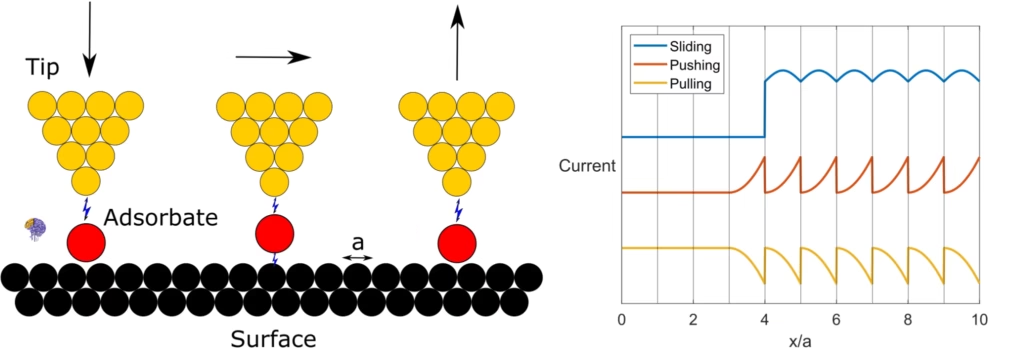
“This figure shows the sequence of steps for moving individual atoms sideways, along with the schematic electrical signals (tunneling current) that correspond to these lateral movements. Note that the current signals have been separated vertically to make them easier to compare.” [20]
The STM was more than just a passive imaging device; it was a tool that could interact with the atomic landscape it observed. This potential was realized in a landmark 1989 experiment that became an iconic moment in the history of science. At IBM’s Almaden Research Center in California, physicists Donald Eigler and Erhard Schweizer used a custom-built, low-temperature STM to achieve the ultimate demonstration of control over matter [5].
Working in an ultra-high vacuum and cooled to just four degrees above absolute zero, they found they could use the STM tip to precisely pick up, move, and place individual xenon atoms on a nickel crystal surface [6]. Over the course of 22 painstaking hours, they arranged 35 xenon atoms to spell out their company’s three-letter logo: “I B M”[2]. This was the definitive fulfillment of Richard Feynman’s 1959 vision of “arranging the atoms one by one the way we want them.” The image of the atomic-scale logo made headlines worldwide, capturing the public’s imagination and providing irrefutable proof that humanity had entered the age of nanotechnology. The STM was not just a “Rosetta Stone” for reading the language of atoms; it was now a pen for writing in it.
The Atomic Force Microscope (AFM): Extending the Reach
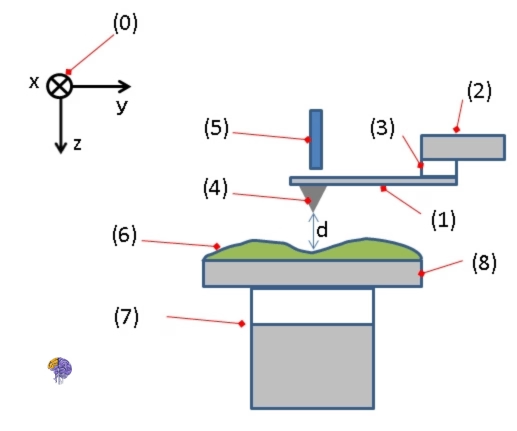
The standard components of an AFM setup are as follows:
1. Cantilever: The primary spring-like element that holds the probe. 2. Cantilever Support: The fixture that secures the cantilever in place. 3. Piezoelectric Element: Used to make the cantilever vibrate at its characteristic frequency. 4. Tip (Probe): A sharp sensor attached to the cantilever’s free end, which interacts with the sample surface. 5. Deflection and Motion Detector: The system responsible for monitoring and measuring the cantilever’s bending and movement. 6. Sample: The material being scanned and analyzed by the AFM. 7. xyz Drive: A mechanism used to precisely control the sample’s position in three dimensions (x, y, and z) relative to the tip. 8. Stage: The platform upon which the sample is placed for scanning. [21]
Despite its revolutionary power, the STM had one significant limitation: it could only be used on conductive or semiconductive samples, as it relied on an electrical current [7]. This excluded a vast universe of materials, including most ceramics, polymers, and, critically, biological molecules. To overcome this, Gerd Binnig, along with Calvin Quate of Stanford University and his IBM colleague Christoph Gerber, developed a new instrument in 1986: the Atomic Force Microscope (AFM) [2].
The AFM operates on a more universal principle: force. It works much like a nanoscale record player or a person reading Braille[1]. A very sharp tip, located at the end of a tiny, flexible cantilever, is scanned across the sample’s surface [8]. As the tip encounters the atomic contours of the surface, weak interatomic forces (such as van der Waals forces) between the tip and the sample cause the cantilever to deflect [9]. This minuscule deflection is measured with incredible precision by reflecting a laser beam off the back of the cantilever and onto a position-sensitive photodiode. By recording the cantilever’s deflection as the tip is scanned, a high-resolution topographic map of the surface can be generated [9].
Because the AFM measures mechanical force rather than electrical current, it can image virtually any type of surface, whether it is conductive or insulating, hard or soft, in air, vacuum, or even liquid [9]. This versatility was a monumental breakthrough. It threw open the doors of nanotechnology to researchers in countless other fields. Biologists could now image single DNA molecules, watch proteins fold, and observe living cells in their natural aqueous environment [10]. Materials scientists could study polymers, glasses, and ceramics with atomic resolution. If the STM opened the door to nanotechnology for physicists and chemists, the AFM “democratized” the nanoscale, making it accessible to the entire scientific community and cementing scanning probe microscopy as a foundational toolkit for modern science.
Section 4: The Carbon Age: Discovery of Fullerenes, Nanotubes, and Graphene

Armed with the new tools to see and manipulate the atomic world, scientists in the 1980s and 1990s embarked on a period of fervent discovery. This era was dominated by a single element: carbon. For centuries, it was believed that pure carbon existed in only two main forms, or allotropes: graphite, the soft, layered material in pencils, and diamond, the hardest substance known. This long-held doctrine was shattered by a series of discoveries that unveiled a whole new family of carbon nanostructures. These discoveries were often serendipitous, emerging from the byproducts of other experiments, and were critically dependent on the advanced analytical technologies of the time. The new carbon allotropes—fullerenes, nanotubes, and later graphene—would become the iconic building blocks of the nanotechnology revolution, promising extraordinary properties and a vast range of applications.
Buckminsterfullerene (C60): The "Buckyball"
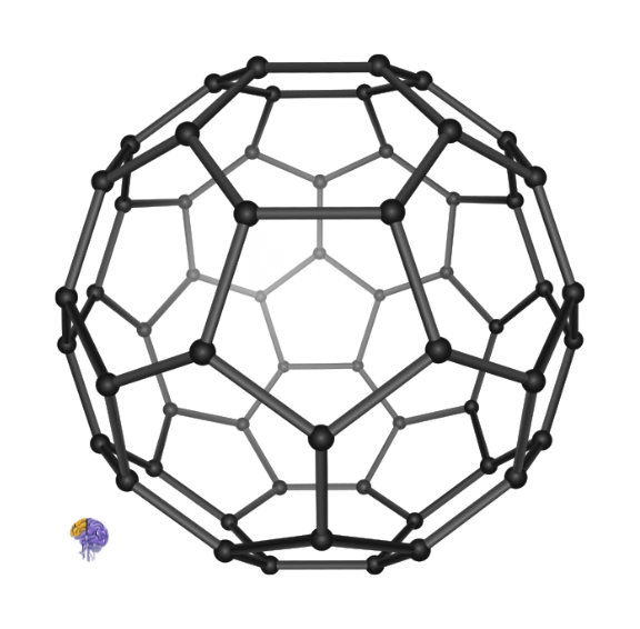
Buckminsterfullerene[22]
The first of these new carbon forms was discovered in 1985 at Rice University in a now-famous 11-day series of experiments [11]. A team led by British chemist Harold Kroto and American chemists Richard Smalley and Robert Curl was using a powerful laser-supersonic cluster beam apparatus, designed by Smalley, to vaporize graphite [12]. Their original goal was to simulate and study the formation of long carbon chains that Kroto had helped discover in interstellar space and the atmospheres of carbon-rich stars [13].
As they analyzed the clusters of carbon atoms formed in the experiment using a mass spectrometer, they noticed a surprisingly strong and persistent peak corresponding to a molecule with exactly 60 carbon atoms (C60) [15]. This molecule was remarkably stable, suggesting a unique and highly symmetric structure. After a period of intense brainstorming and model-building (including Smalley famously using paper, scissors, and tape to construct a model at home), the team proposed a radical structure: a hollow sphere resembling a soccer ball [14]. The structure, a truncated icosahedron, consisted of 20 hexagonal faces and 12 pentagonal faces, with a carbon atom at each of the 60 vertices [11]. They named this elegant new molecule “buckminsterfullerene” in honor of the architect R. Buckminster Fuller, whose geodesic domes shared the same geometric principles [11].
The discovery, published in the journal Nature, announced the existence of a third major form of pure carbon [11]. It was a monumental finding that opened an entirely new branch of chemistry. For their pioneering work, Kroto, Smalley, and Curl were awarded the 1996 Nobel Prize in Chemistry [3]. The “buckyball,” as it was nicknamed, became the first member of a new class of molecules known as fullerenes.
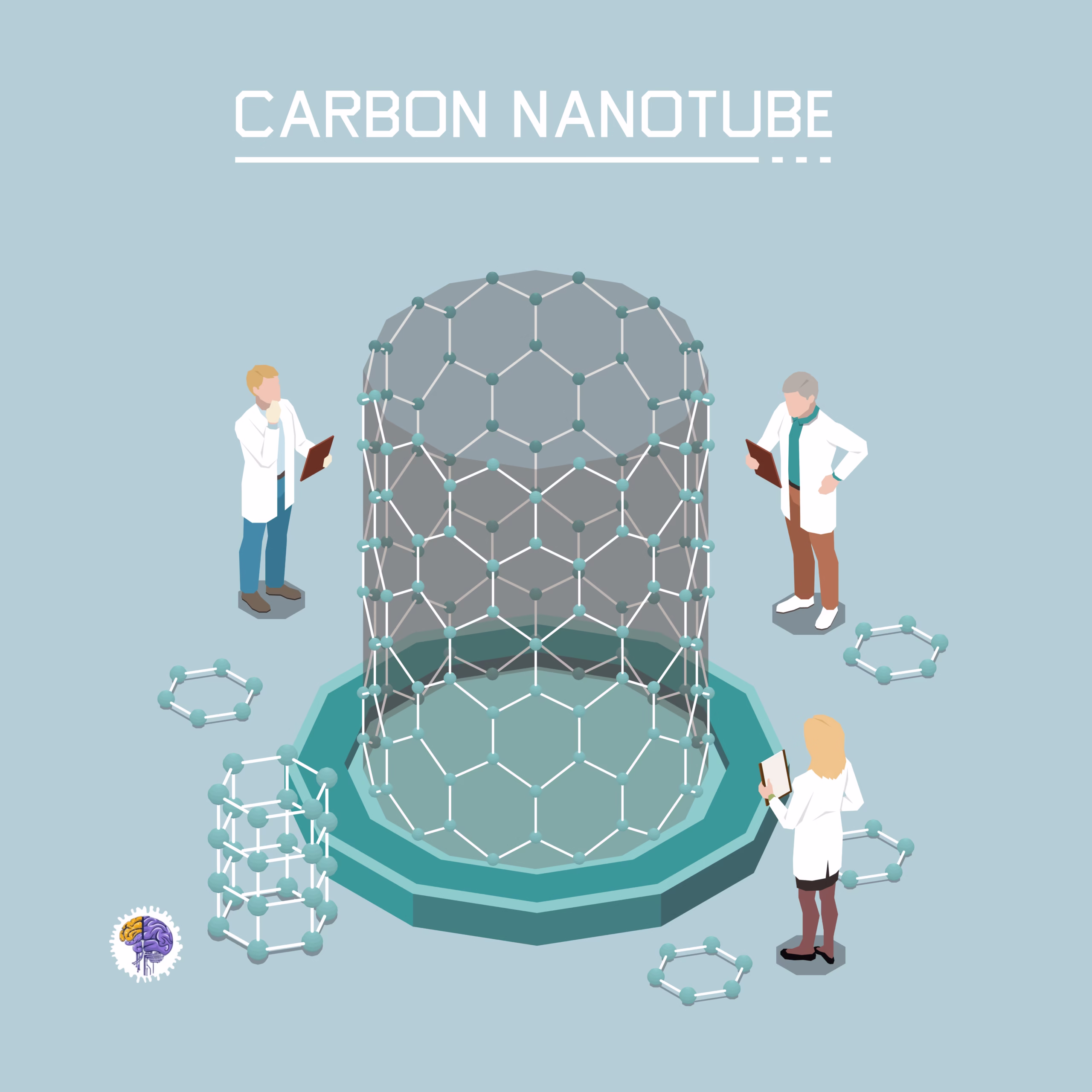
Carbon Nanotubes (CNTs): The Pillars of Nanotechnology
Carbon Nanotubes (CNTs): The Pillars of NanotechnologyThe first of these new carbon forms was discovered in 1985 at Rice University in a now-famous 11-day series of experiments [11]. A team led by British chemist Harold Kroto and American chemists Richard Smalley and Robert Curl was using a powerful laser-supersonic cluster beam apparatus, designed by Smalley, to vaporize graphite [12]. Their original goal was to simulate and study the formation of long carbon chains that Kroto had helped discover in interstellar space and the atmospheres of carbon-rich stars [13].
Iijima’s paper, also published in Nature, is widely credited with igniting the global research effort into CNTs [16]. It is important to note, however, that “discovery” is often a complex social and scientific process. Earlier, overlooked observations of hollow carbon filaments had been made as far back as 1952 by Soviet scientists Radushkevich and Lukyanovich, and later by Morinobu Endo in 1976 and others [17]. However, these findings occurred before the scientific community was prepared to understand their significance. Iijima’s 1991 report came at the perfect moment—in the wake of the buckyball discovery and with the rise of nanotechnology as a field—and his clear elucidation of their structure served as the true catalyst for the research explosion.
Scientists quickly found that CNTs possessed a suite of extraordinary properties. They exhibited a tensile strength approximately 100 times that of steel at only one-sixth the weight, along with exceptional electrical and thermal conductivity [18]. In 1993, research accelerated further when Iijima’s group and a separate group at IBM led by Donald Bethune independently developed methods to produce single-walled carbon nanotubes (SWCNTs), which consist of a single rolled-up graphene sheet [17]. These remarkable properties established CNTs as one of the most promising and heavily studied materials in the entire field of nanotechnology.
Graphene: The Two-Dimensional Wonder Material
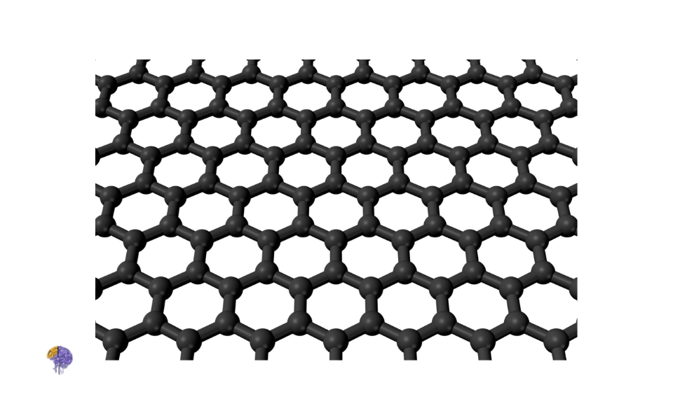
Graphene[23]
For years, scientists had theorized about graphene—a single, flat, one-atom-thick sheet of carbon atoms arranged in a honeycomb lattice—but it was widely believed to be too unstable to exist in a free state. This belief was overturned in 2004 by Andre Geim and Konstantin Novoselov at the University of Manchester[2]. Using a surprisingly low-tech method, they succeeded in isolating single layers of graphene. They applied a piece of ordinary Scotch tape to a block of graphite and peeled it away, then repeatedly peeled the tape against itself, progressively thinning the graphite flakes until they were left with sheets that were just a single atom thick[2].
The properties of this new 2D material were even more astounding than those of CNTs. Graphene was found to be the strongest material ever measured, an incredibly efficient conductor of heat and electricity, and almost completely transparent. The discovery opened up a vast new area of research into two-dimensional materials. In recognition of their “groundbreaking experiments,” Geim and Novoselov were awarded the 2010 Nobel Prize in Physics, just six years after their initial publication—an exceptionally rapid acknowledgment of the discovery’s transformative impact[2]. Together, the discoveries of fullerenes, nanotubes, and graphene defined the “carbon age” of nanotechnology, providing a versatile and powerful toolkit of nanomaterials that continues to drive innovation today.
Conclusion
In retrospect, the period spanning from the early 1980s to the mid-2000s marks the definitive birth of experimental nanotechnology. The developments detailed were not merely incremental advances but paradigm-shifting breakthroughs that fundamentally altered humanity’s relationship with matter. The invention of the Scanning Tunneling and Atomic Force Microscopes provided more than just images; they established an entirely new methodology for exploring and engineering the physical world at its most fundamental level. This transformation from passive observation to active manipulation was powerfully symbolized by the “I B M” logo, demonstrating that the atomic frontier was now a canvas for human creation. This newfound power directly enabled the “Carbon Age,” where the discoveries of fullerenes, nanotubes, and graphene shattered long-held scientific dogmas and introduced a trio of materials with properties that seemed to defy previous limits. Together, the development of these revolutionary tools and the discovery of these iconic nanomaterials formed a symbiotic relationship that propelled nanotechnology from a speculative vision into a vibrant and essential field of modern science, laying the groundwork for the countless innovations that continue to emerge today.
Clarifying the Concepts
1. Why couldn't scientists see individual atoms with traditional microscopes?
2. How is the Lycurgus Cu2. What is a Scanning Tunneling Microscope (STM) and how does it work?p an example of ancient nanotechnology?
3. What was the significance of the 1989 "I B M" logo experiment?
4. What is an Atomic Force Microscope (AFM) and how is it different from an STM?
5. What is the main advantage of the AFM over the STM?
6. What is a "buckyball" and why was its discovery in 1985 important?
7. What are carbon nanotubes (CNTs)?
8. What is graphene and what makes it a "wonder material"?
Reference
[1]. September 1981: Invention of the scanning tunneling microscope – This Month in Physics History | American Physical Society, accessed on September 25, 2025, https://www.aps.org/publications/apsnews/200308/history.cfm
[2]. 1.2 Historical Development and Milestones in Nanotechnology – Fiveable, accessed on September 25, 2025, https://fiveable.me/introduction-nanotechnology/unit-1/historical-development-milestones-nanotechnology/study-guide/U28ogmx53wvhvFfT
[3]. History of nanotechnology – Wikipedia, accessed on September 25, 2025, https://en.wikipedia.org/wiki/History_of_nanotechnology
[4]. Scanning Tunneling Microscopy (STM): An Overview – Oxford Instruments Asylum Research, accessed on September 25, 2025, https://afm.oxinst.com/modes/scanning-tunneling-microscopy-stm
[5]. Scanning tunneling microscope – IBM, accessed on September 25, 2025, https://www.ibm.com/history/scanning-tunneling-microscope
[6]. Nanotechnology – IBM, accessed on September 25, 2025, https://www.ibm.com/history/nanotechnology
[7]. Lecture 1 Scanning Tunneling and Atomic Force Microscopies Principles – SOEST Hawaii, accessed on September 25, 2025, http://www.soest.hawaii.edu/HIGP/Faculty/sksharma/GG711/GG711Lec04AFM.pdf
[8]. Atomic force microscopy – Wikipedia, accessed on September 25, 2025, https://en.wikipedia.org/wiki/Atomic_force_microscopy
[9]. Atomic Force Microscopy (AFM): All you need to know – NanoMagnetics Instruments, accessed on September 25, 2025, https://www.nanomagnetics-inst.com/post/atomic-force-microscopy-blogpost
[10]. Changing Our View of the Nanoscale World | The Kavli Prize, accessed on September 25, 2025, https://www.kavliprize.org/changing-our-view-of-the-nanoscale-world
[11]. Fullerene | Definition, Properties, Uses, & Facts – Britannica, accessed on September 25, 2025, https://www.britannica.com/science/fullerene
[12]. Press release: The 1996 Nobel Prize in Chemistry – NobelPrize.org, accessed on September 25, 2025, https://www.nobelprize.org/prizes/chemistry/1996/press-release/
[13]. Discovery of Fullerenes National Historic Chemical Landmark, accessed on September 25, 2025, https://www.acs.org/education/whatischemistry/landmarks/fullerenes.html
[14]. Discovery of Fullerenes – American Chemical Society, accessed on September 25, 2025, https://www.acs.org/content/dam/acsorg/education/whatischemistry/landmarks/lesson-plans/discovery-of-fullerenes.pdf
[15]. Buckminsterfullerene – Wikipedia, accessed on September 25, 2025, https://en.wikipedia.org/wiki/Buckminsterfullerene
[16]. Carbon Nanotube Research in Its 30th Year | ACS Nano – ACS Publications, accessed on September 25, 2025, https://pubs.acs.org/doi/10.1021/acsnano.1c04972
[17]. Carbon nanotube – Wikipedia, accessed on September 25, 2025, https://en.wikipedia.org/wiki/Carbon_nanotube
[18]. From Faraday to nanotubes – timeline — Science Learning Hub, accessed on September 25, 2025, https://www.sciencelearn.org.nz/resources/1658-from-faraday-to-nanotubes-timeline
[19]. https://en.wikipedia.org/wiki/Scanning_tunneling_microscope, 9Credit: Michael Schmid and Grzegorz Pietrzak / License: CC BY-SA 2.0 AT)
[20]. https://en.wikipedia.org/wiki/Atomic_manipulation, (Credit: VilamV, Schematics of Vertical manipulation, via Wikimedia Commons / License: CC BY-SA 4.0)
[21]. https://en.wikipedia.org/wiki/Atomic_force_microscopy (Credit: Tom Toyosaki, Typical configuration of AFM, via Wikimedia Commons / License: CC BY-SA 4.0)
[22]. Credit: 傭 / Title: Buckminsterfullerene C60 / License: CC BY-SA 4.0
[23]. Credit: Jynto / Title: Ball-and-stick model of graphene / License: CC BY-SA 4.0